Call us now :08045802968

 Send Inquiry
SMT Stencil
Price 100-100000 INR/ Piece
MOQ : 100 Pieces
SMT Stencil Specification
- Style
- Modern Arts
- Usage & Applications
- SMT Solder Paste Printing, Electronics Manufacturing
- Features
- Laser Cut, Reusable, Durable
- Control Type
- Manual
- Regional Style
- Other
- Material
- Other
- Product Type
- Other
- Feature
- High Precision Apertures
- Finishing
- Other
- Technique
- Other
- Wood Type
- Other
- Fabric Type
- Other
- Finish Type
- Electropolished
- Theme
- Other
- Color
- any colour
- Metals Type
- Other
- Weight
- Lightweight
- Size
- Customizable
- Shape
- Rectangular
- Mesh Type
- Stainless Steel Frame Supported
- Aperture Tolerance
- ±0.01 mm
- Cleaning
- Solvent Washable
- Stencil Thickness
- 0.1 mm to 0.2 mm (typical)
- Surface Treatment
- Anti-solder Ball
- Application Compatibility
- Compatible with All Major SMT Printers
- Packing Type
- Safe Carton/Protection Box
SMT Stencil Trade Information
- Minimum Order Quantity
- 100 Pieces
- Supply Ability
- 10000 Pieces Per Day
- Delivery Time
- 1 Week
- Sample Available
- Yes
- Sample Policy
- Free samples are available
- Main Domestic Market
- Manipur, Dadra and Nagar Haveli, Chandigarh, Himachal Pradesh, Pondicherry, Uttarakhand, Daman and Diu, , South India, North India, East India, West India, Andaman and Nicobar Islands, Assam, Arunachal Pradesh, Bihar, Delhi, Goa, Haryana, Jammu and Kashmir, Jharkhand, Kerala, Madhya Pradesh, Maharashtra, Mizoram, Meghalaya, Nagaland, Punjab, Rajasthan, Sikkim, Tamil Nadu, Telangana, Tripura, West Bengal, Lakshadweep, Uttar Pradesh, Gujarat, Karnataka, Andhra Pradesh, Central India, Odisha, Chhattisgarh, All India
About SMT Stencil
SMT Stencil as specially laser cut solder peste stencils which can be provided separately or permanently mounted in a stencil frame by sun acrylam pvt. ltd.f frame stencils are designed for high volume screen printing on printed circuit boards, framed SMT stencils can be used for 16 MIL pitch and below and for Micro BGA's. main feature of SMT STENCILS unique process for smooth aperture walls very clean cut apertures excellent print performance excellent for high-volume stencil printing on printed circuit boards unique process creates permanent non- removable non- fading.
Precision Engineering for Reliable Results
Crafted with high-precision laser cutting, our SMT stencil guarantees consistently accurate solder paste depositions. The 0.01 mm aperture tolerance, coupled with a customizable rectangular frame, offers versatility for a wide range of boards and components. This ensures your electronics assembly delivers dependable outcomes every time.
Advanced Surface Treatment for Defect Reduction
The anti-solder ball surface treatment significantly reduces common soldering issues, promoting cleaner joints and minimizing rework. The electropolished finish creates a smooth interface, further enhancing performance and increasing stencil lifespan. Maintain productivity while reducing waste and defects in your assembly line.
Versatile and Easy to Maintain
Compatible with all major SMT printers, our stencil is engineered for flexibility. Its solvent washable design simplifies cleaning and maintenance, while robust packaging ensures safe arrival. Lightweight and durable, this reusable stencil supports both Bluetooth and manual control systems, accommodating diverse manufacturing needs.
FAQ's of SMT Stencil:
Q: How does the anti-solder ball surface treatment benefit my SMT process?
A: The anti-solder ball surface treatment helps minimize solder balls during the reflow process, resulting in cleaner solder joints, reduced defects, and fewer post-assembly touchups. This treatment enhances overall production yield and reliability.Q: What is the recommended cleaning method for this SMT stencil?
A: This stencil is designed to be solvent washable, allowing easy removal of solder paste residues. Regular cleaning with an appropriate solvent maintains precise aperture definition and prolongs the stencil's service life.Q: When should I consider using a stencil with 0.1 mm versus 0.2 mm thickness?
A: Stencil thickness selection depends on your specific component and solder paste requirements. Thinner stencils (around 0.1 mm) are ideal for fine-pitch components, while thicker stencils (up to 0.2 mm) are often preferred for larger pads or when higher paste volumes are necessary.Q: Where can I use this stencil within an electronics manufacturing setup?
A: This stencil is compatible with all major SMT printers, making it suitable for any standard surface mount technology production line, whether in small-batch prototyping or high-volume manufacturing environments.Q: What process is used to achieve high precision in stencil apertures?
A: Apertures are laser-cut with state-of-the-art technology, ensuring precision with a tolerance of 0.01 mm. This method guarantees uniform paste deposits and optimal printing consistency across multiple production cycles.Q: How can I customize the stencil's size, shape, or color for my application?
A: You can specify required dimensions, rectangular shapes, and color preferences when ordering. The product is customizable to fit your unique board design and branding needs.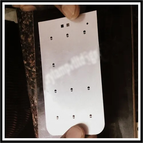
Tell us about your requirement

Price:
Quantity
Select Unit
- 50
- 100
- 200
- 250
- 500
- 1000+
Additional detail
Mobile number
Email

More Products in Metal Letter Stencil Category
Metal Letter Stencil
Price 100 INR / Piece
Minimum Order Quantity : 100 Pieces
Metals Type : Metal
Theme : Love
Color : any colour
Height : any Millimeter (mm)
Our Products
- Acrylic Sheet
- Laser Cutting Designs
- Laser Cutting Services
- Bakelite Sheet
- PVC Foam Sheets
- Switch Board Sheet
- Compac Sheets
- Fabric Sheet
- Hylam Sheet
- P1 Sheet
- Acrylic Mirror Sheets
- Acrylic Laser Cutting Job Work
- Cartoon Wall Decor
- Wall Stencils
- Acrylic Pipe
- LED Diffuser Sheet
- Acrylic Light Guide Plate
- Acrylic Plastic Sheet
- Letter Stencil
- Metal Letter Stencil
- Basket Ball Back Board.
- Transparent Sheet
- Cast Acrylic Sheet
- HPL Sheet
- High Pressure Laminate Sheet
- Acrylic Mobile Stand
- Acrylic keychain
- Acrylic Book Holder
- Acrylic Laboratory Equipement
- Acrylic Photo Frame
- Acrylic Certificate Holder
- Acrylic Numbers
- Acrylic Watch
- Acrylic CD/DVD Display
- Acrylic Jwellery Display
- Acrylic Table Calander
- Acrylic Paper Holder
- Photo Frame Acrylic
- Acrylic Clear Glass photo Frame
- Acrylic Golden Mirror Invitation Card Sheet
- Acrylic Silver Mirror Invitation Card Sheet
- Marriage Invitation crad Acrylic Sheet.
- Acrylic Box Display for Building Model Sheet
- CNC Glass Cutting Machine
- Automatic Glass Cutting Machine
- Glass Circle Cutting Machine
- Mirror Glass Cutting Machine
- 1 MM Mirror Glass Cutting Machine
- Multi Head Glass Cutting Machine
- Circle cutting machine
- Plastic Coin
- Sunpack sheet
- Plastic Token
- Acrylic Tube
- Craft Materials
- Light Diffusion Sheet
- Acrylic Sheet Fabrication Services
- POCKET BADGES


2 Number, Lati Bazar Zone ( Vibhag) - 2, B/h Gita Mandir, Nr. S.T.Bus Depot, Ahmedabad - 380022, Gujarat, India

Mr Nikesh Shah
(Chief Operating Officer)
Mobile :08045802968
 Send Inquiry
 Send SMS
Developed and Managed by Infocom Network Private Limited.
